- 您现在的位置:买卖IC网 > Sheet目录473 > MAX2851ITK+ (Maxim Integrated)TRANSMITTER MIMO 5GHZ 5CH 68TQFN
5GHz, 5-Channel MIMO Receiver
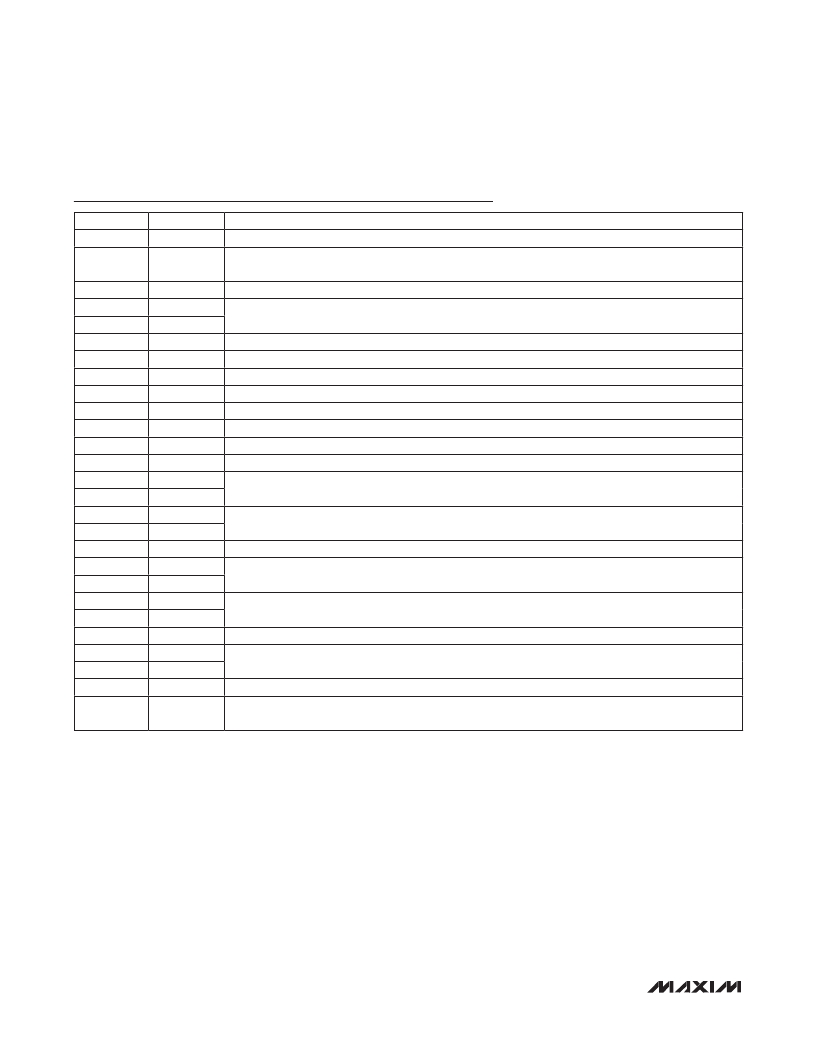
Pin Description (continued)
PIN
43
44
45
46
47
48
49
50
51
52
53
54
55
56
57
58
59
60
61
62
63
64
65
66
67
68
—
NAME
V CC_VCO
BYP_VCO
GND_VCO
CPOUT+
CPOUT-
V CC_DIG
DOUT
CLKOUT2
CLKOUT
V CC_XTAL
XTAL
XTAL_CAP
RSSI
RXBBI2+
RXBBI2-
RXBBQ2+
RXBBQ2-
V CC_BB1
RXBBI1+
RXBBI1-
RXBBQ1+
RXBBQ1-
V CC_LNA1
RXRF1+
RXRF1-
ENABLE
EP
FUNCTION
VCO Supply Voltage. Bypass with a capacitor as close as possible to the pin.
On-Chip VCO Regulator Output Bypass. Bypass with an external 1 F F capacitor to GND_VCO with
minimum PCB trace. Do not connect other circuitry to this pin.
VCO Ground
Differential Charge-Pump Output. Connect the frequency synthesizer’s loop filter between
CPOUT+ and CPOUT- (see the Typical Operating Circuit ).
Digital Block Supply Voltage. Bypass with a capacitor as close as possible to the pin.
Data Logic Output of 4-Wire Serial Interface
Reference Clock Buffer Output 2
Reference Clock Buffer Output
Crystal Oscillator Supply Voltage. Bypass with a capacitor as close as possible to the pin.
Crystal Oscillator Base Input. AC-couple crystal unit to this pin.
Crystal Oscillator Emitter Node
Receiver Signal Strength Indicator Output
Receiver 2 Baseband I-Channel Differential Output
Receiver 2 Baseband Q-Channel Differential Output
Receiver Baseband Supply Voltage 1. Bypass with a capacitor as close as possible to the pin.
Receiver 1 Baseband I-Channel Differential Output
Receiver 1 Baseband Q-Channel Differential Output
Receiver 1 LNA Supply Voltage. Bypass with a capacitor as close as possible to the pin.
Receiver 1 LNA Differential Input. Input is DC-coupled and biased internally at 1.2V.
Enable Logic Input
Exposed Paddle. Connect to the ground plane with multiple vias for proper operation and heat
dissipation. Do not share with any other pin grounds and bypass capacitors’ ground.
22
_____________________________________________________________________________________
发布紧急采购,3分钟左右您将得到回复。
相关PDF资料
MAX2852ITK+
IC RECEIVER DFS 5GHZ 68TQFN
MAX2870EVKIT#
EVAL KIT MAX2870
MAX2904EVKIT
EVAL KIT
MAX3524EVKIT
EVAL KIT MAX3524
MAX3540EVKIT#
KIT FOR MAX3540 DVB TUNER
MAX3541EVKIT+
KIT FOR MAX3541 DVB TUNER
MAX3542CLM+
IC TV TUNER SGL CONV 48LFCGA
MAX3542EVKIT+
KIT FOR MAX3542 DVB TUNER
相关代理商/技术参数
MAX2851ITK+T
功能描述:射频接收器 RF and RFID 射频接收器s - TRANSMITTER MIMO 5GHZ 5CH 68TQFN RoHS:否 制造商:Skyworks Solutions, Inc. 类型:GPS Receiver 封装 / 箱体:QFN-24 工作频率:4.092 MHz 工作电源电压:3.3 V 封装:Reel
MAX2852ITK+
功能描述:射频接收器 5Ghz Receiver RoHS:否 制造商:Skyworks Solutions, Inc. 类型:GPS Receiver 封装 / 箱体:QFN-24 工作频率:4.092 MHz 工作电源电压:3.3 V 封装:Reel
MAX2852ITK+T
功能描述:射频接收器 5Ghz Receiver RoHS:否 制造商:Skyworks Solutions, Inc. 类型:GPS Receiver 封装 / 箱体:QFN-24 工作频率:4.092 MHz 工作电源电压:3.3 V 封装:Reel
MAX2870ETJ+
功能描述:锁相环 - PLL PLL/VCO RoHS:否 制造商:Silicon Labs 类型:PLL Clock Multiplier 电路数量:1 最大输入频率:710 MHz 最小输入频率:0.002 MHz 输出频率范围:0.002 MHz to 808 MHz 电源电压-最大:3.63 V 电源电压-最小:1.71 V 最大工作温度:+ 85 C 最小工作温度:- 40 C 封装 / 箱体:QFN-36 封装:Tray
MAX2870ETJ+T
功能描述:锁相环 - PLL PLL/VCO RoHS:否 制造商:Silicon Labs 类型:PLL Clock Multiplier 电路数量:1 最大输入频率:710 MHz 最小输入频率:0.002 MHz 输出频率范围:0.002 MHz to 808 MHz 电源电压-最大:3.63 V 电源电压-最小:1.71 V 最大工作温度:+ 85 C 最小工作温度:- 40 C 封装 / 箱体:QFN-36 封装:Tray
MAX2870EVKIT#
功能描述:射频开发工具 MAX2870 Eval Kit RoHS:否 制造商:Taiyo Yuden 产品:Wireless Modules 类型:Wireless Audio 工具用于评估:WYSAAVDX7 频率: 工作电源电压:3.4 V to 5.5 V
MAX2880ETP+
制造商:Maxim Integrated Products 功能描述:12.4GHZ HIGH PERFORMANCE FRACTIONAL/INTEGER-N SYNTHESIZER - Rail/Tube 制造商:Maxim Integrated Products 功能描述:RF FRACT INTEGER N SYNTH QFN
MAX2880ETP+T
制造商:Maxim Integrated Products 功能描述:RF FRACT INTEGER N SYNTH QFN
